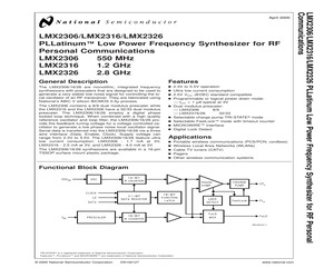
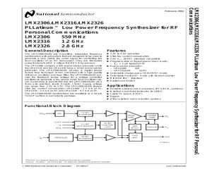
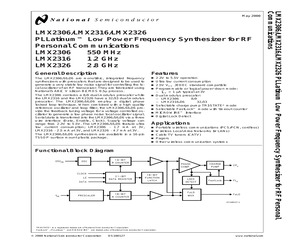
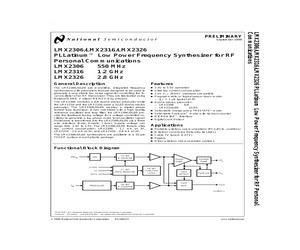
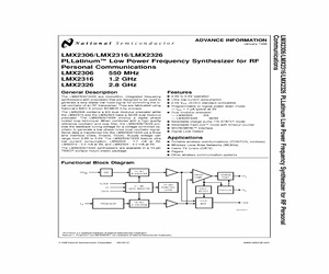
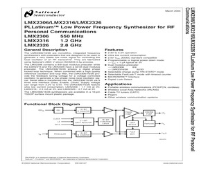
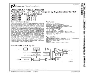
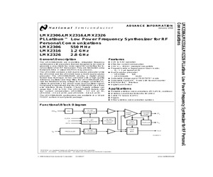
Synthesizer for RF Personal Communications April 2000 LMX2306/LMX2316/LMX2326 Connection Diagrams LMX2306/16/26 LMX2306/16/26 DS100127-2 DS100127-19 16-Lead (0.173" Wide) Thin Shrink Small Outline Package(TM) Order Number LMX2306TM, LMX2306TMX, LMX2316TM, LMX2316TMX, LMX2326TM or LMX2326TMX See NS Package Number MTC16 16-pin Chip Scale Package Order Number LMX2306SLBX, LMX2316SLBX or LM2326SLBX See NS Package Number SLB16A Pin Descriptions 16-Pin 16-Pin TSSOP CSP Pin I/O Name Description 1 15 FLo O FastLock Output. For connection of parallel resistor to the loop filter. (See Section 1.3.4 FASTLOCK MODES description.) 2 16 CPo O Charge Pump Output. For connection to a loop filter for driving the input of an external VCO. 3 1 GND 4 2 GND 5 3 fIN I RF Prescaler Complementary Input. A bypass capacitor should be placed as close as possible to this pin and be connected directly to the ground plane. The complementary input can be left unbypassed, with some degradation in RF sensitivity. 6 4 fIN I RF Pre
 19 Pages, 278 KB, Original
um Low Power Frequency Synthesizer for RF Personal Communications PRELIMINARY Connection Diagrams LMX2306/16/26 LMX2306/16/26 DS100127-2 DS100127-19 16-Lead (0.173" Wide) Thin Shrink Small Outline Package(TM) Order Number LMX2306TM, LMX2306TMX, LMX2316TM, LMX2316TMX, LMX2326TM or LMX2326TMX See NS Package Number MTC16 16-pin Chip Scale Package Order Number LMX2306SLBX, LMX2316SLBX or LM2326SLBX See NS Package Number SLB16A Pin Descriptions 16-Pin 16-Pin TSSOP CSP 1 15 Pin I/O Name Description FLo O FastLock Output. For connection of parallel resistor to the loop filter. (See Section 1.3.4 FASTLOCK MODES description.) O Charge Pump Output. For connection to a loop filter for driving the input of an external VCO. 2 16 CPo 3 1 GND 4 2 GND 5 3 fIN I RF Prescaler Complementary Input. A bypass capacitor should be placed as close as possible to this pin and be connected directly to the ground plane. The complementary input can be left unbypassed, with some degradation in RF sensitivity. 6 4 fIN I RF Pre
 19 Pages, 280 KB, Original
306/LMX2316/LMX2326 PLLatinum Low Power Frequency Synthesizer for RF Personal Communications PRELIMINARY Connection Diagram LMX2306/16/26 DS100127-2 16-Lead (0.173" Wide) Thin Shrink Small Outline Package(TM) Order Number LMX2306TM, LMX2306TMX, LMX2316TM, LMX2316TMX, LMX2326TM or LMX2326TMX See NS Package Number MTC16 Pin Description 16-Pin 1 Pin Name I/O FLo O FastLock Output. For connection of parallel resistor to the loop filter. (See Section 1.3.4 FASTLOCK MODES description.) O Charge Pump Output. For connection to a loop filter for driving the input of an external VCO. 2 CPo 3 GND 4 GND 5 fIN I I 6 fIN 7 VCC1 8 OSCIN 9 Description Charge Pump Ground. Analog Ground. RF Prescaler Complementary Input. A bypass capacitor should be placed as close as possible to this pin and be connected directly to the ground plane. The complementary input can be left unbypassed, with some degradation in RF sensitivity. RF Prescaler Input. Small signal input from the VCO. Analog Power Supply Voltage Input. Input
 18 Pages, 248 KB, Original
26 FL, 41 O 16F-V, cP, -42 15 Voce GND 43 14. Fo/LD GND 4 13, LE _ TOP VIEW fy 75 12; Data fin 76 11 f- Clock Vee 7 10, CE OSCy ] 8 9> GND DS100127-2 16-Lead (0.173 Wide) Thin Shrink Small Outline Package(TM) Order Number LMX2306TM, LMX2306TMX, LMX2316TM, LMX2316TMX, LMX2326TM or LMX2326TMX See NS Package Number MTC16 Pin Descriptions LMX2306/16/26 cP, Fly Vp Oe F,/LD a a} Veg2 Top View tw) [4] Data Vee | [] [9] | Clock S%in ono DS100127-19 16-pin Chip Scale Package Order Number LMX2306SLBX, LMX2316SLBX or LM2326SLBX See NS Package Number SLB16A 16-Pin |16-Pin Pin |/O Description SSOP | CSP | Name 4 15 FL, O | FastLock Output. For connection of parallel resistor to the loop filter. (See Section 1.3.4 FASTLOCK MODES description.) 2 16 CP, O | Charge Pump Output. For connection to a loop filter for driving the input of an external VCO. 3 4 GND Charge Pump Ground. 4 2 GND Analog Ground. 5 3 fin | | RF Prescaler Complementary Input. A bypass capacitor should be placed as close as possible to this pin
 19 Pages, 927 KB, Scan
thesizer for RF Personal Communications February 2002 LMX2306/LMX2316/LMX2326 Connection Diagrams LMX2306/16/26 LMX2306/16/26 DS100127-2 DS100127-19 16-Lead (0.173" Wide) Thin Shrink Small Outline Package(TM) Order Number LMX2306TM, LMX2306TMX, LMX2316TM, LMX2316TMX, LMX2326TM or LMX2326TMX See NS Package Number MTC16 16-pin Chip Scale Package Order Number LMX2306SLBX, LMX2316SLBX or LM2326SLBX See NS Package Number SLB16A Pin Descriptions 16-Pin 16-Pin TSSOP CSP 1 15 Pin I/O Name Description FLo O FastLock Output. For connection of parallel resistor to the loop filter. (See Section 1.3.4 FASTLOCK MODES description.) O Charge Pump Output. For connection to a loop filter for driving the input of an external VCO. 2 16 CPo 3 1 GND Charge Pump Ground. 4 2 GND Analog Ground. 5 3 fIN I RF Prescaler Complementary Input. A bypass capacitor should be placed as close as possible to this pin and be connected directly to the ground plane. The complementary input can be left unbypassed, with some degradation
 19 Pages, 278 KB, Original
y Synthesizer for RF Personal Communications May 2000 LMX2306/LMX2316/LMX2326 Connection Diagrams LMX2306/16/26 LMX2306/16/26 DS100127-2 DS100127-19 16-Lead (0.173" Wide) Thin Shrink Small Outline Package(TM) Order Number LMX2306TM, LMX2306TMX, LMX2316TM, LMX2316TMX, LMX2326TM or LMX2326TMX See NS Package Number MTC16 16-pin Chip Scale Package Order Number LMX2306SLBX, LMX2316SLBX or LM2326SLBX See NS Package Number SLB16A Pin Descriptions 16-Pin 16-Pin TSSOP CSP Pin I/O Name Description 1 15 FLo O FastLock Output. For connection of parallel resistor to the loop filter. (See Section 1.3.4 FASTLOCK MODES description.) 2 16 CPo O Charge Pump Output. For connection to a loop filter for driving the input of an external VCO. 3 1 GND 4 2 GND 5 3 fIN I RF Prescaler Complementary Input. A bypass capacitor should be placed as close as possible to this pin and be connected directly to the ground plane. The complementary input can be left unbypassed, with some degradation in RF sensitivity. 6 4 fIN I RF Pre
 25 Pages, 316 KB, Original
y Synthesizer for RF Personal Communications May 2000 LMX2306/LMX2316/LMX2326 Connection Diagrams LMX2306/16/26 LMX2306/16/26 DS100127-2 DS100127-19 16-Lead (0.173" Wide) Thin Shrink Small Outline Package(TM) Order Number LMX2306TM, LMX2306TMX, LMX2316TM, LMX2316TMX, LMX2326TM or LMX2326TMX See NS Package Number MTC16 16-pin Chip Scale Package Order Number LMX2306SLBX, LMX2316SLBX or LM2326SLBX See NS Package Number SLB16A Pin Descriptions 16-Pin 16-Pin TSSOP CSP Pin I/O Name Description 1 15 FLo O FastLock Output. For connection of parallel resistor to the loop filter. (See Section 1.3.4 FASTLOCK MODES description.) 2 16 CPo O Charge Pump Output. For connection to a loop filter for driving the input of an external VCO. 3 1 GND 4 2 GND 5 3 fIN I RF Prescaler Complementary Input. A bypass capacitor should be placed as close as possible to this pin and be connected directly to the ground plane. The complementary input can be left unbypassed, with some degradation in RF sensitivity. 6 4 fIN I RF Pre
 19 Pages, 278 KB, Original
y Synthesizer for RF Personal Communications May 2002 LMX2306/LMX2316/LMX2326 Connection Diagrams LMX2306/16/26 LMX2306/16/26 DS100127-2 DS100127-19 16-Lead (0.173" Wide) Thin Shrink Small Outline Package(TM) Order Number LMX2306TM, LMX2306TMX, LMX2316TM, LMX2316TMX, LMX2326TM or LMX2326TMX See NS Package Number MTC16 16-pin Chip Scale Package Order Number LMX2306SLBX, LMX2316SLBX or LM2326SLBX See NS Package Number SLB16A Pin Descriptions 16-Pin 16-Pin TSSOP CSP 1 15 Pin I/O Name Description FLo O FastLock Output. For connection of parallel resistor to the loop filter. (See Section 1.3.4 FASTLOCK MODES description.) O Charge Pump Output. For connection to a loop filter for driving the input of an external VCO. 2 16 CPo 3 1 GND Charge Pump Ground. 4 2 GND Analog Ground. 5 3 fIN I RF Prescaler Complementary Input. A bypass capacitor should be placed as close as possible to this pin and be connected directly to the ground plane. The complementary input can be left unbypassed, with some degradation
 19 Pages, 279 KB, Original
um Low Power Frequency Synthesizer for RF Personal Communications PRELIMINARY Connection Diagrams LMX2306/16/26 LMX2306/16/26 DS100127-2 DS100127-19 16-Lead (0.173" Wide) Thin Shrink Small Outline Package(TM) Order Number LMX2306TM, LMX2306TMX, LMX2316TM, LMX2316TMX, LMX2326TM or LMX2326TMX See NS Package Number MTC16 16-pin Chip Scale Package Order Number LMX2306SLBX, LMX2316SLBX or LM2326SLBX See NS Package Number SLB16A Pin Descriptions 16-Pin 16-Pin TSSOP CSP 1 15 Pin I/O Name Description FLo O FastLock Output. For connection of parallel resistor to the loop filter. (See Section 1.3.4 FASTLOCK MODES description.) O Charge Pump Output. For connection to a loop filter for driving the input of an external VCO. 2 16 CPo 3 1 GND 4 2 GND 5 3 fIN I RF Prescaler Complementary Input. A bypass capacitor should be placed as close as possible to this pin and be connected directly to the ground plane. The complementary input can be left unbypassed, with some degradation in RF sensitivity. 6 4 fIN I RF Pre
 19 Pages, 280 KB, Original
 LMX2306/16/26 FL, 1 16 Vv, cP, 42 15 Veen GND 3 14} Fo/LD GND 4 3 LE _ TOP VIEW fin 5 12} Data fn 8 11 Clock Vee1 47 10} CE OSCy 48 9 GND DS100127-2 16-Lead (0.173 Wide) Thin Shrink Small Outline Package(TM) Order Number LMX2306TM, LMX2306TMX, LMX2316TM, LMX2316TMX, LMX2326TM or LMX2326TMX See NS Package Number MTC16 Pin Description 16-Pin Pin vo Description Name 1 FL 0 FastLock Output. For connection of parallel resistor to the loop filter. (See Section 1.3.4 FASTLOCK MODES description.) 2 CP, 0 Charge Pump Output. For connection to a loop filter for driving the input of an external VCO. 3 GND Charge Pump Ground. 4 GND Analog Ground. 5 fin RF Prescaler Complementary Input. A bypass capacitor should be placed as close as possible to this pin and be connected directly to the ground plane. The complementary input can be left unbypassed, with some degradation in RF sensitivity. 6 fin RF Prescaler Input. Small signal input from the VCO. Voc Analog Power Supply Voltage Input. Input may range from 2.3
 18 Pages, 564 KB, Scan
306/16/26 LMX2306/16/26 10012719 10012702 16-pin Chip Scale Package Order Number LMX2306SLBX, LMX2316SLBX or LM2326SLBX See NS Package Number SLB16A 16-Lead (0.173" Wide) Thin Shrink Small Outline Package(TM) Order Number LMX2306TM, LMX2306TMX, LMX2316TM, LMX2316TMX, LMX2326TM or LMX2326TMX See NS Package Number MTC16 Pin Descriptions 16-Pin 16-Pin TSSOP CSP Pin Name I/O Description FLo O FastLock Output. For connection of parallel resistor to the loop filter. (See Section 1.3.4 FASTLOCK MODES description.) 16 CPo O Charge Pump Output. For connection to a loop filter for driving the input of an external VCO. 1 GND 4 2 GND 5 3 fIN I RF Prescaler Complementary Input. A bypass capacitor should be placed as close as possible to this pin and be connected directly to the ground plane. The complementary input can be left unbypassed, with some degradation in RF sensitivity. 6 4 fIN I RF Prescaler Input. Small signal input from the VCO. 7 5 VCC1 8 6 OSCIN 1 15 2 3 Charge Pump Ground. Analog Ground. Analog
 19 Pages, 317 KB, Original
LMX2306/16/26 LMX2306/16/26 10012719 10012702 16-pin Chip Scale Package Order Number LMX2306SLBX, LMX2316SLBX or LM2326SLBX See NS Package Number SLB16A 16-Lead (0.173" Wide) Thin Shrink Small Outline Pkg(TM) Order Number LMX2306TM, LMX2306TMX, LMX2316TM, LMX2316TMX, LMX2326TM or LMX2326TMX See NS Package Number MTC16 Pin Descriptions 16-Pin 16-Pin TSSOP CSP 1 15 2 3 Pin Name I/O Description FLo O FastLock Output. For connection of parallel resistor to the loop filter. (See Section 1.3.4 FASTLOCK MODES description.) 16 CPo O Charge Pump Output. For connection to a loop filter for driving the input of an external VCO. 1 GND Charge Pump Ground. 4 2 GND Analog Ground. 5 3 fIN I RF Prescaler Complementary Input. A bypass capacitor should be placed as close as possible to this pin and be connected directly to the ground plane. The complementary input can be left unbypassed, with some degradation in RF sensitivity. 6 4 fIN I RF Prescaler Input. Small signal input from the VCO. 7 5 VCC1 8 6 OSCIN Analog
 22 Pages, 367 KB, Original
Synthesizer for RF Personal Communications April 2001 LMX2306/LMX2316/LMX2326 Connection Diagrams LMX2306/16/26 LMX2306/16/26 DS100127-2 DS100127-19 16-Lead (0.173" Wide) Thin Shrink Small Outline Package(TM) Order Number LMX2306TM, LMX2306TMX, LMX2316TM, LMX2316TMX, LMX2326TM or LMX2326TMX See NS Package Number MTC16 16-pin Chip Scale Package Order Number LMX2306SLBX, LMX2316SLBX or LM2326SLBX See NS Package Number SLB16A Pin Descriptions 16-Pin 16-Pin TSSOP CSP 1 15 Pin I/O Name Description FLo O FastLock Output. For connection of parallel resistor to the loop filter. (See Section 1.3.4 FASTLOCK MODES description.) O Charge Pump Output. For connection to a loop filter for driving the input of an external VCO. 2 16 CPo 3 1 GND Charge Pump Ground. 4 2 GND Analog Ground. 5 3 fIN I RF Prescaler Complementary Input. A bypass capacitor should be placed as close as possible to this pin and be connected directly to the ground plane. The complementary input can be left unbypassed, with some degradation
 19 Pages, 278 KB, Original
316/LMX2326 PLLatinum Low Power Frequency Synthesizer for RF Personal Communications ADVANCE INFORMATION Connection Diagram LMX2306/16/26 DS100127-2 16-Lead (0.173" Wide) Thin Shrink Small Outline Package(TM) Order Number LMX2306TM, LMX2306TMX, LMX2316TM, LMX2316TMX, LMX2326TM or LMX2326TMX See NS Package Number MTC16 Pin Description 16-Pin 1 Pin Name I/O FLo O FastLock Output. For connection of parallel resistor to the loop filter. (See Section 1.3.4 FASTLOCK MODES description.) O Charge Pump Output. For connection to a loop filter for driving the input of an external VCO. 2 CPo 3 GND 4 GND 5 fIN I I 6 fIN 7 VCC1 8 OSCIN 9 Description Charge Pump Ground. Analog Ground. RF Prescaler Complementary Input. A bypass capacitor should be placed as close as possible to this pin and be connected directly to the ground plane. The complementary input can be left unbypassed, with some degradation in RF sensitivity. RF Prescaler Input. Small signal input from the VCO. Analog Power Supply Voltage Input. Input
 18 Pages, 248 KB, Original
thesizer for RF Personal Communications December 2000 LMX2306/LMX2316/LMX2326 Connection Diagrams LMX2306/16/26 LMX2306/16/26 DS100127-2 DS100127-19 16-Lead (0.173" Wide) Thin Shrink Small Outline Package(TM) Order Number LMX2306TM, LMX2306TMX, LMX2316TM, LMX2316TMX, LMX2326TM or LMX2326TMX See NS Package Number MTC16 16-pin Chip Scale Package Order Number LMX2306SLBX, LMX2316SLBX or LM2326SLBX See NS Package Number SLB16A Pin Descriptions 16-Pin 16-Pin TSSOP CSP Pin I/O Name Description 1 15 FLo O FastLock Output. For connection of parallel resistor to the loop filter. (See Section 1.3.4 FASTLOCK MODES description.) 2 16 CPo O Charge Pump Output. For connection to a loop filter for driving the input of an external VCO. 3 1 GND 4 2 GND 5 3 fIN I RF Prescaler Complementary Input. A bypass capacitor should be placed as close as possible to this pin and be connected directly to the ground plane. The complementary input can be left unbypassed, with some degradation in RF sensitivity. 6 4 fIN I RF Pre
 22 Pages, 295 KB, Original


