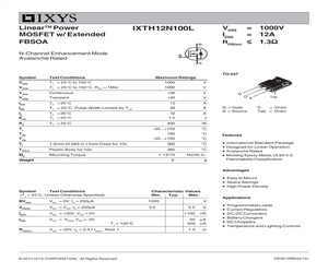
IXTH12N100L LinearTM Power MOSFET w/ Extended FBSOA VDSS ID25 RDS(on) = 1000V = 12A 1.3 N-Channel Enhancement Mode Avalanche Rated TO-247 Symbol Test Conditions Maximum Ratings VDSS TJ = 25C to 150C 1000 V VDGR TJ = 25C to 150C, RGS = 1M 1000 V VGSS Continuous 30 V VGSM Transient 40 V ID25 TC = 25C 12 A IDM TC = 25C, Pulse Width Limited by TJM 25 A IA EAS TC = 25C TC = 25C 12 1.5 A J PD TC = 25C 400 W -55...+150 C TJM 150 C Tstg -55...+150 C TJ TL 1.6mm (0.063 in.) from Case for 10s 300 C TSOLD Plastic Body for 10s 260 C Md Mounting Torque 1.13/10 Nm/lb.in. 6 g Weight G D Tab S G = Gate S = Source D = Drain Tab = Drain Features * International Standard Package * Designed for Linear Operation * Avalanche Rated * Molding Epoxy Meets UL94 V-0 Flammability Classification Advantages * Easy to Mount * Space Savings * High Power Density Symbol Test Conditions (TJ = 25C, Unless Otherwise Specified) Characteristic Values Min. Typ. Max. BVDSS VGS = 0V, ID = 250A 1000 VGS(th) VDS = VGS, ID = 250A 3.5 IGSS V
 6 Pages, 143 KB, Original
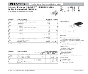
IXTH12N100L With Extended FBSOA VDSS ID25 N-Channel Enhancement Mode RDS(on) Symbol Test Conditions VDSS TJ = 25C to 150C 1000 V VDGR TJ = 25C to 150C; RGS = 1 M 1000 V VGS Continuous 30 V VGSM Transient 40 V ID25 TC = 25C 12 A IDM TC = 25C, pulse width limited by TJM 25 A IAR TC = 25C 12 A EAR TC = 25C V A Maximum Ratings TO-247 (IXTH) (TAB) 30 mJ 1.5 J 400 W -55 to +150 C TJM 150 C Features Tstg -55 to +150 C z EAS PD = 1000 = 12 1.3 TC = 25C TJ G = Gate D = Drain S = Source TAB = Drain TL 1.6 mm (0.063 in) from case for 10 s 300 C z TSOLD Plastic body for 10 s 260 C z Md Mounting torque 0.9/7.9 Nm/lb.in. Weight TO-247 6 g Designed for linear operation International standard package Unclamped Inductive switching (UIS) rated z Molding epoxies meet UL 94 V-0 flammability classification Applications z z Symbol Test Conditions Characteristic Values (TJ = 25C, unless otherwise specified) Min. Typ. Max. BVDSS VGS = 0 V, ID = 250 A 1000 VGS(th) VDS = VGS, ID = 250 A 3 IGSS VGS = 30 V, VDS = 0 V IDSS V
 5 Pages, 81 KB, Original
IXTH12N100L LinearTM Power MOSFET w/ Extended FBSOA VDSS ID25 RDS(on) = 1000V = 12A 1.3 N-Channel Enhancement Mode Avalanche Rated TO-247 Symbol Test Conditions Maximum Ratings VDSS TJ = 25C to 150C 1000 V VDGR TJ = 25C to 150C, RGS = 1M 1000 V VGSS Continuous 30 V VGSM Transient 40 V ID25 TC = 25C 12 A IDM TC = 25C, Pulse Width Limited by TJM 25 A IA EAS TC = 25C TC = 25C 12 1.5 A J PD TC = 25C 400 W -55...+150 C TJM 150 C Tstg -55...+150 C TJ TL 1.6mm (0.063 in.) from Case for 10s 300 C TSOLD Plastic Body for 10s 260 C Md Mounting Torque 1.13/10 Nm/lb.in. 6 g Weight G D Tab S G = Gate S = Source D = Drain Tab = Drain Features * International Standard Package * Designed for Linear Operation * Avalanche Rated * Molding Epoxy Meets UL94 V-0 Flammability Classification Advantages * Easy to Mount * Space Savings * High Power Density Symbol Test Conditions (TJ = 25C, Unless Otherwise Specified) Characteristic Values Min. Typ. Max. BVDSS VGS = 0V, ID = 250A 1000 VGS(th) VDS = VGS, ID = 250A 3.5 IGSS V
 5 Pages, 145 KB, Original
IXTH12N100L With Extended FBSOA VDSS ID25 N-Channel Enhancement Mode RDS(on) Symbol Test Conditions VDSS TJ = 25C to 150C 1000 V VDGR TJ = 25C to 150C; RGS = 1 M 1000 V VGS Continuous 30 V VGSM Transient 40 V ID25 TC = 25C 12 A IDM TC = 25C, pulse width limited by TJM 25 A IAR TC = 25C 12 A EAR TC = 25C V A Maximum Ratings TO-247 (IXTH) (TAB) 30 mJ 1.5 J 400 W -55 to +150 C TJM 150 C Features Tstg -55 to +150 C z EAS PD = 1000 = 12 1.3 TC = 25C TJ G = Gate D = Drain S = Source TAB = Drain TL 1.6 mm (0.063 in) from case for 10 s 300 C z TSOLD Plastic body for 10 s 260 C z Md Mounting torque 0.9/7.9 Nm/lb.in. Weight TO-247 6 g Designed for linear operation International standard package Unclamped Inductive switching (UIS) rated z Molding epoxies meet UL 94 V-0 flammability classification Applications z z Symbol Test Conditions Characteristic Values (TJ = 25C, unless otherwise specified) Min. Typ. Max. BVDSS VGS = 0 V, ID = 250 A 1000 VGS(th) VDS = VGS, ID = 250 A 3 IGSS VGS = 30 V, VDS = 0 V IDSS V
 6 Pages, 85 KB, Original
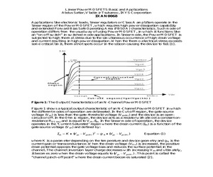
Id = 0.6A IXTN46N50L 500 46 0.18 240 SOT-227B @ V ds = 400V, Id = 0.6A IXTK46N50L 500 46 0.18 240 TO-264 @ V ds = 400V, Id = 0.6A IXTN62N50L 500 62 0.156 300 SOT-227B @ V ds = 400V, I d = 0.75A IXTB62N50L 500 62 0.156 300 PLUS264 @ V ds = 400V, Id = 0.75A IXTH12N100L 1000 12 0.31 200 TO-247 @ V ds = 600V, Id = 0.25A IXTX22N100L 1000 24 0.18 240 PLUS247 @ V ds = 800V, Id = 0.3A IXTN22N100L 1000 24 0.18 240 SOT-227B @ V ds = 800V, Id = 0.3A, IXTK22N100L 1000 24 0.18 240 TO-264 @ V ds = 800V, Id = 0.3A IXTN30N100L 1000 30 0.156 300 SOT-227B @ V ds = 600V, Id = 0.5A IXTB30N100L 1000 30 0.156 300 PLUS264 @ V ds = 600V, Id = 0.5A Based on equation (2), a single power MOSFET such as IXTK22N100L with voltage rating of 1000V provides a power rating of 700W. This power rating is normally used in the circuit design for switch-mode operation but not for linear applications. For linear operation, IXYS provides a Safe Operating Area (SOA) rating that is obtained under a strict DC operation condition such as 24
 7 Pages, 493 KB, Original
0V overvoltage is a constant DC voltage for 10ms. This duration exceeds Mil-Std-1275 which specifies a 70s surge to 250V that decays in 1.6ms. Using the following equation (based on charging with 9A) to set the CT: CT = IT * t 2.5ms = 9A * 8.2nF V 2.8V M1 IXTH12N100L VIN 160V (RECTIFIED 110V AC) 100V TO 800V VOUT 0.5A (200V CLAMP) CG 2nF RG 10 RIN 4.64M R1 470k SD R2 100k Q1 BF722 VDD C1 0.47F GATE LTC4366-2 SD TIMER VSS OUT FB BASE RFB1 12.4k RFB2 2M CT 3.3nF DANGER! Lethal Voltages Present RSS 412k 436612 F07 Figure 7. Rectified 110V AC Supply Protected from 220V AC 436612fe For more information www.linear.com/LTC4366 19 LTC4366 APPLICATIONS INFORMATION 28V Vehicle Application The circuit in Figure 8 adds reverse voltage protection to the standard 28V application shown in Figure 6. There are three modes to this circuit: pass FET On when the input is 18V to 41V, clamping the output to 43V when more than 43V appears at the input and finally reverse voltage protection when up to -250V DC is presen
 24 Pages, 286 KB, Original
IXTC26N50P IXTC280N055T IXTC36P15P IXTC62N15P IXTC72N30T IXTC75N10 IXTD5N100A IXTE250N10 IXTF200N10T IXTF230N085T IXTF250N075T IXTF280N055T IXTH102N15T IXTH102N20T IXTH102N25T IXTH10P50P IXTH10P60 IXTH110N10L2 IXTH110N25T IXTH11P50 IXTH120P065T IXTH12N100 IXTH12N100L PART NUMBER (WKS) CF CF CF 8 CF 8 8 CF 8 8 8 8 8 8 8 8 CF 8 8 8 8 8 8 8 CF 8 CF CF 8 8 8 8 8 CF CF 8 CF 10 CF 8 8 10 CF IXTH12N100Q IXTH12N120 IXTH130N10T IXTH130N15T IXTH130N20T IXTH13N110 IXTH13N80 IXTH140P05T IXTH14N100 IXTH14N80 IXTH150N17T IXTH152N085T IXTH15N50L2 IXTH160N075T IXTH160N10T IXTH160N15T IXTH16N10D2 IXTH16N20D2 IXTH16N50D2 IXTH16P20 IXTH16P60P IXTH180N085T IXTH180N10T IXTH182N055T IXTH1N100 IXTH1N250 IXTH200N075T IXTH200N085T IXTH200N10T IXTH20N60 IXTH20P50P IXTH21N50 IXTH220N055T IXTH220N075T IXTH22N50P IXTH230N085T IXTH240N055T IXTH24N50 IXTH24N50L IXTH24P20 IXTH24P20-7B IXTH250N075T IXTH260N055T2 CF 8 8 8 8 6 4 8 6 4 8 8 8 8 8 8 8 10 8 CF 8 8 8 8 CF CF 8 8 8 8 8 4 8 CF 8 8 8 4 CF 8 8 8 8 GmbH - Lead Time Guide PA
 16 Pages, 65 KB, Original
50V overvoltage is a constant DC voltage for 10ms. This duration exceeds Mil-Std-1275 which specifies a 70s surge to 250V that decays in 1.6ms. Using the following equation (based on charging with 9A) to set the CT: CT = IT * 2.5ms t = 9A * 10nF V 2.5V M1 IXTH12N100L VIN 160V (RECTIFIED 110V AC) 100V TO 800V VOUT 0.5A (200V CLAMP) CG 2nF RG 10 RIN 4.64M R1 470k SD R2 100k Q1 BF722 VDD C1 0.47F GATE LTC4366-2 SD TIMER VSS OUT FB BASE RFB1 12.4k RFB2 2M CT 3.3nF DANGER! Lethal Voltages Present RSS 412k 436612 F07 Figure 7. Rectified 110V AC Supply Protected from 220V AC 436612fd For more information www.linear.com/LTC4366 19 LTC4366-1/LTC4366-2 Applications Information 28V Vehicle Application The circuit in Figure 8 adds reverse voltage protection to the standard 28V application shown in Figure 6. There are three modes to this circuit: pass FET On when the input is 18V to 41V, clamping the output to 43V when more than 43V appears at the input and finally reverse voltage protection when up to -250V
 24 Pages, 287 KB, Original
50V overvoltage is a constant DC voltage for 10ms. This duration exceeds Mil-Std-1275 which specifies a 70s surge to 250V that decays in 1.6ms. Using the following equation (based on charging with 9A) to set the CT: CT = IT * t 2.5ms = 9A * 10nF V 2.5V M1 IXTH12N100L VIN 160V (RECTIFIED 110V AC) 100V TO 800V VOUT 0.5A (200V CLAMP) CG 2nF RG 10 RIN 4.64M R1 470k SD R2 100k Q1 BF722 VDD C1 0.47F GATE LTC4366-2 SD TIMER VSS OUT FB BASE RFB1 12.4k RFB2 2M CT 3.3nF DANGER! Lethal Voltages Present RSS 412k 436612 F07 Figure 7. Rectified 110V AC Supply Protected from 220V AC 436612fc 19 LTC4366-1/LTC4366-2 APPLICATIONS INFORMATION 28V Vehicle Application The circuit in Figure 8 adds reverse voltage protection to the standard 28V application shown in Figure 6. There are three modes to this circuit: pass FET On when the input is 18V to 41V, clamping the output to 43V when more than 43V appears at the input and finally reverse voltage protection when up to -250V DC is present at the input. The reverse volt
 24 Pages, 227 KB, Original


